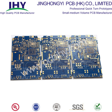
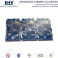
HDI Printed Circuit Boards
HDI Printed Circuit Boards, one of the fastest growing technologies in PCBs, are now available at JHY PCB. HDI Boards contain blind and/or buried vias and often contain microvias of .006 or less in diameter. They have a higher circuitry density than traditional circuit boards.
There are 6 different types of HDI Printed Circuit Boards, through vias from surface to surface, with buried vias and through vias, two or more HDI layer with through vias, passive substrate with no electrical connection, coreless construction using layer pairs and alternate constructions of coreless constructions using layer pairs.
The most common 6 types of HDI Printed Circuit Boards include:
- Through vias from surface-to-surface
- Combination through vias and buried vias
- Multiple HDI layers containing through vias
- A passive mounting substrate without any electrical connections
- Coreless construction through the use of layer pairs
- Alternate coreless constructions through the use of layer pairs

HDI Printed Circuit Board
The attributes of the displayed product
| Type | HDI PCB |
| Layers | 8L |
| Base Material | IT180 |
| Dielectric | Prepreg |
| Board Thickness | 1.6mm±10% |
| Copper Weight | 1oz |
| Surface Finish | ENIG 2U" |
| Minimum trace Width/Spacing | 0.1/0.1mm(4/4mils) |
| Solder Mask Color | Blue |
| Silkscreen Color | White |
| Min. Hole Size | 0.1mm |
| Via in Pad | Yes |
| Epoxy Via Plug | Yes |
| Hole Copper Wall Thickness | 25.4um |
| Controlled Impedance | Yes |
| Flame Retardant Properties | 94 V-0 |
| Application | Industrial Controllers |
HDI Printed Circuit Boards Structures:
1) HDI PCB (1+N+1)
Features:
- Suitable for BGA with lower I/O counts
- Fine line, microvia and registration technologies capable of 0.4 mm ball pitch
- Qualified material and surface treatment for Lead-free process
- Excellent mounting stability and reliability
- Copper filled via
Application: Cell phone, UMPC, MP3 Player, PMP, GPS, Memory Card
1+N+1 HDI PCB Structure:
2) HDI PCB (2+N+2)
Features:
- Suitable for BGA with smaller ball pitch and higher I/O counts
- Increase routing density in complicated design
- Thin board capabilities
- Lower Dk / Df material enables better signal transmission performance
- Copper filled via
Application: Cell phone, PDA, UMPC, Portable game console, DSC, Camcorder
2+N+2 HDI PCB Structure:

3) ELIC (Every Layer Interconnection)
Features:
- Every layer via structure maximizes design freedom
- Copper filled via provides better reliability
- Superior electrical characteristics
- Cu bump and metal paste technologies for very thin board
Application: Cell phone, UMPC, MP3, PMP, GPS, Memory card.
Every Layer Interconnection Structure:

Advanced Capabilities: Microvias PCB A microvia maintains a laser drilled diameter of typically 0.006" (150µm), 0.005" (125µm), or 0.004" (100µm), which are optically aligned and require a pad diameter typically 0.012" (300µm), 0.010" (250µm), or 0.008" (200µm), allowing additional routing density. Microvias can be via-in-pad, offset, staggered or stacked, non-conductive filled and copper plated over the top or solid copper filled or plated. Microvias add value when routing out of fine pitch BGAs (BGA PCB) such as 0.8 mm pitch devices and below. Additionally, microvias add value when routing out of a 0.5 mm pitch device where staggered microvias can be used, however, routing micro-BGAs such as 0.4 mm, 0.3 mm, or 0.25 mm pitch device, requires the use of Stacked MicroVias using an inverted pyramid routing technique. JHY PCB maintains years of experience with HDI products and was a pioneer of second generation microvias or Stacked MicroVias. Stacked MicroVias Technology offers solid copper stacked microvias providing rout-out solutions for micro BGAs. JHY PCB developed and now offer an entire family of microvia technology solutions for your next generation products. The list below shows JHY PCB's entire family of Microvia Technology. Standard or First Generation Microvias - Create routing density (eliminate through vias)
- Reduce layer count
- Enhance electrical characteristics
- Standard Microvias limited to layers 1 - 2 & 1 - 3
Stacked MicroVias or Second Generation Microvias - Allows increased routing on multiple layers - multilayer PCB
- Provides routing solutions for next generation applications
- 1 mm - 0.8 mm - 0.65 mm - 0.5 mm - 0.4 mm - 0.3 mm & 0.25 mm
- Provides solid copper plate eliminating potential solder voiding
- Provides a Thermal Management Solution
- Improves Current Carrying Capability
- Improves Current Carrying Capability
- Provides a Planar surface for BGA (Via-in-Pad)
- Allows any layer via technology
Deep Microvias - Provide additional dielectric material & small geometry features.
- Improved Impedance performance - Impedance Control PCB
- Provides RF Microvia solutions
- Provides a solid copper plate
- Improves Current Carrying Capability & Thermal Management
- Provides a Planar surface for BGA (Via-in-Pad)
Deep Stacked MicroVias - Provides additional dielectric for RF applications
- Maintains small geometries on multiple layers
- Improved signal integrity
- Provides a solid copper plate
- Improves Current Carrying Capability & Thermal Management
- Provides a Planar surface for BGA (Via-in-Pad)
Any layer HDI - Multilayer copper filled stacked micro via structure
- 1.2/1.2 mil line/space
- 4/8 mil laser via capture pad size
- Material options:
- High temperature FR4
- Halogen - Free
- High Speed (low loss)
Benefits of using HDI Printed Circuit Boards As consumer demands change, so must technology. By using HDI technology, designers now have the option to place more components on both sides of the raw PCB. Multiple via processes, including via in pad and blind via technology, allow designers more PCB real estate to place components that are smaller even closer together. Decreased component size and pitch allow for more I/O in smaller geometries. This means faster transmission of signals and a significant reduction in signal loss and crossing delays. HDI Printed Circuit Boards fabrication manufacturer HDI Printed Circuit Boards, one of the fastest growing technologies in PCBs, are now available at JHY PCB whatever PCB Prototyping or Express HDI PCB .HDI Boards contain blind and/or buried vias and often contain microvias of .006 or less in diameter. Find a HDI PCB Manufacturer and Supplier. Choose Quality HDI PCB Manufacturers, Suppliers, Exporters at pcbjhy.com.Welcome to send your design to us. Contact us if you need more details on HDI Printed Circuit Boards. We are ready to answer your questions on packaging, logistics, certification or any other aspects about HDI PCB Board、HDI PCB Factory. If these products fail to match your need, please contact us and we would like to provide relevant information.
Product Categories : HDI PCB